
Tata Semiconductor Dholera: Current Status, Fab Details & Production Plans

Key Highlights
Tata Semiconductor Dholera is an approximately ₹91,000 crore semiconductor fabrication facility being developed by Tata Electronics at Dholera SIR, Gujarat. The 300 mm fab is planned to process up to 50,000 wafers per month and support semiconductor technologies ranging from 28nm to 110nm.
The project is one of the most important industrial developments in Dholera and is intended to support India's growing semiconductor manufacturing ecosystem.
Tata Semiconductor Dholera: Key Facts
- Company: Tata Electronics
- Location: Dholera SIR, Gujarat
- Investment: Approximately ₹91,000 crore
- Fab type: 300 mm / 12-inch semiconductor fabrication facility
- Planned capacity: Up to 50,000 wafers per month
- Technology: 28nm to 110nm
- Technology partner: PSMC, Taiwan
- SEZ area: 66.166 hectares
- Government-estimated employment potential: Approximately 21,000 people
- Current status: Under development and progressing toward operational readiness
The Government of India approved the Dholera fab in February 2024, while the dedicated 66.166-hectare Tata Semiconductor SEZ in Dholera was notified in April 2026.
What is the Tata Semiconductor Plant in Dholera?
The Tata semiconductor plant in Dholera is a front end semiconductor fabrication facility, commonly called a fab.
This means the facility will manufacture semiconductor circuits directly on silicon wafers rather than only assembling or packaging finished chips.
Tata Electronics describes the Dholera facility as an AI-enabled 300 mm foundry being developed with technology support from Taiwan's Powerchip Semiconductor Manufacturing Corporation (PSMC).
What is the Current Status of Tata Semiconductor Dholera?
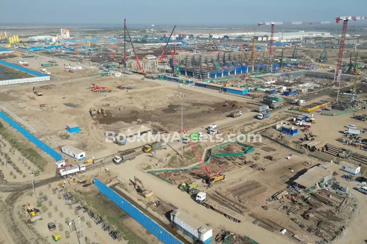
As of September 2026, the Tata Electronics Dholera fab project is 50% complete, remains under development, and is not yet commercially operational.
Tata Electronics has said that the project is progressing toward operational readiness. The company is working with engineering, equipment, materials and supply-chain partners to prepare the facility for semiconductor manufacturing.
In September 2026, Tata Electronics announced a collaboration with Kelington to deploy critical infrastructure and systems required for semiconductor production. The partnership is intended to support the fab's operational readiness for silicon wafer production.
What Technology will the Dholera Fab Use?
The Dholera semiconductor fab is designed to support process technologies ranging from 28nm to 110nm.
Tata Electronics currently lists:
- 28nm
- 40nm
- 55nm
- 90nm
- 110nm
These technologies can support a wide range of semiconductor products rather than only one type of chip.
What Chips will Tata Manufacture in Dholera?
The Tata Electronics Dholera fab is planned to manufacture analog and logic semiconductor products such as:
- Power management ICs
- Microcontrollers
- Display drivers
- High-performance computing logic
These chips can serve industries including:
- Automotive and electric vehicles
- Artificial intelligence
- Computing and data storage
- Wireless communication
- Consumer electronics
- Internet of Things
- Mobile devices
Tata Electronics says the foundry is being developed to serve customers in India and international markets.
What does 50,000 Wafers Per Month Mean?
The planned capacity of 50,000 wafers per month does not mean the plant will manufacture only 50,000 chips.
A semiconductor fab processes large silicon wafers, and each wafer can contain many individual chip dies depending on the size and design of the semiconductor.
The 50,000 figure therefore describes the fab's planned wafer-processing capacity, not the number of individual chips produced.
What is a 300 mm Semiconductor Fab?
A 300 mm fab manufactures semiconductor circuits on silicon wafers approximately 300 millimetres, or 12 inches, in diameter.
Larger wafers allow manufacturers to produce many semiconductor dies on a single wafer and are commonly used for high-volume semiconductor manufacturing.
Tata describes Dholera as India's first commercial 300 mm semiconductor fab.
Key Technology, Equipment and Supply-Chain Partners
The Dholera fab is being supported by a growing network of global semiconductor companies.
| Partner | Main Role |
|---|---|
| PSMC | Semiconductor process technology and manufacturing support |
| ASML | Lithography equipment, solutions and fab ramp-up support |
| Tokyo Electron | Semiconductor manufacturing equipment and workforce training |
| Synopsys | Process technology, design platform and design enablement |
| Fujifilm | Advanced semiconductor materials |
| Sumitomo Chemical | High-purity semiconductor materials |
| Sojitz & NRS | Critical materials supply, storage and logistics |
| Kelington | Fab infrastructure and operational-readiness systems |
One of the most important equipment partnerships is the Tata Electronics–ASML collaboration, which covers lithography solutions and support for the establishment and ramp-up of the Dholera fab.
Tata Electronics has also expanded its materials, infrastructure and supply-chain network through multiple semiconductor partnerships announced around SEMICON India 2026.
Together, these partnerships cover semiconductor technology, equipment, materials, design, engineering, logistics and operational readiness.
Tata Semiconductor SEZ in Dholera
In April 2026, the Government of India notified a dedicated Special Economic Zone for Tata Semiconductor Manufacturing Private Limited in Dholera.
The SEZ covers 66.166 hectares and is designed to support electronic hardware, software and related operations.
The government estimated employment potential of approximately 21,000 people from the SEZ development.
The SEZ provides a formal industrial and regulatory framework around one of Dholera's largest manufacturing projects.
When will the Tata Semiconductor Plant Start Production?
The Tata semiconductor plant start date has not yet been officially confirmed as a commercial production date.
As of September 2026, the fab remains under development, with Tata Electronics and its partners preparing infrastructure and systems required for wafer production.
Before a semiconductor fab reaches full commercial manufacturing, it typically moves through stages such as:
- Equipment installation
- Clean-room readiness
- Tool commissioning
- Process qualification
- Trial wafer production
- Production ramp-up
Specific future production dates should therefore be treated as project targets until Tata Electronics formally confirms the start of commercial manufacturing.
Readers tracking how the project has moved from government approval to construction and operational preparation can also follow the Tata Semiconductor Dholera timeline.
Why is Tata Semiconductor Important for Dholera?
The semiconductor fab adds a major high-technology manufacturing industry to Dholera SIR.
Its development can support:
- Skilled employment
- Semiconductor suppliers
- Engineering companies
- Logistics and warehousing
- Technology and workforce training
- Supporting services
- Residential and commercial demand
The fab is also being supported by Dholera's planned industrial infrastructure, including roads, power, water, wastewater systems and digital connectivity.
Beyond the main fab, Tata Electronics expects a much wider supplier ecosystem to develop around the project. A planned 363-acre vendor park and semiconductor supplier ecosystem in Dholera is intended to support companies providing materials, chemicals, engineering, logistics and other specialised services.
However, the fab's development should not be treated as a guarantee of property price growth. Future real-estate demand will depend on actual employment, population growth, infrastructure, location, approvals and wider development around Dholera.
FAQs
Q. Is Tata Semiconductor Dholera operational?
No. As of September 2026, the fab is still under development and is progressing toward operational readiness.
Q. What is the investment in Tata Semiconductor Dholera?
The Tata Electronics semiconductor fab in Dholera involves an investment of approximately ₹91,000 crore.
Q. What is the capacity of the Tata Dholera Fab?
The planned capacity is up to 50,000 semiconductor wafers per month.
Q. Who is Tata's Technology Partner for the Dholera Fab?
Tata Electronics is working with Powerchip Semiconductor Manufacturing Corporation (PSMC) of Taiwan for semiconductor process technology and manufacturing support.
Q. When will Tata Semiconductor Dholera start production?
A confirmed commercial production date has not yet been announced. The fab remains under development, with infrastructure, equipment and operational-readiness work progressing.


